Power Supply

WTI400 v1.2 — In service — installed on test vessel
Overview
This page documents the 3.3 V VCC rail that powers the ESP32 module and all digital logic on the WTI400. The rail is generated by an LMR51610 synchronous buck converter from the protected bus supply (VSD ≈ 12 V), and the SMPS output is then routed through a single ferrite bead (FB1) into the digital VCC domain.
The same KiCad sheet (power_supplies.kicad_sch) also contains the LP2951 LDO that supplies the wind transducer (rails VSC, VAS, signals WND_EN/WND_ERR, ferrite FB2, and jumper JP1). That sub-circuit is documented on the Wind Interface page; this page covers only the SMPS portion.
The four sub-circuits on this page, in narrative order:
- Input stage — VSD bulk capacitance (C2) and high-frequency bypass (C4) at the LMR51610 VIN pin.
- LMR51610 buck converter core — the converter IC, its bootstrap, feedforward, feedback divider, and a Do-Not-Populate snubber footprint.
- Output filter — the inductor L1, two flanking bulk capacitors, and a small 3v3 bypass.
- SMPS → VCC domain boundary — the ferrite bead FB1 that is the sole copper path from the SMPS output rail to the digital VCC distribution.
The layout closely follows the Monolithic Power Systems EMI webinar ("Practical Grounding and Layout") recommendations. Each sub-circuit explanation calls out the specific webinar recommendation the layout matches.
Functional specification and design objectives
The SMPS must convert the protected bus supply into a clean 3.3 V digital rail across the full operating envelope, while keeping switching noise out of the radio and analog sense lines. The page-level objectives are:
- Generate 3.30 V from a 9.0–14.8 V continuous input, tolerating an 18.6 V transient clamp from upstream protection.
- Deliver up to 360 mA continuous to the VCC rail without exceeding the IC junction-temperature limit at 85 °C ambient.
- Filter the 400 kHz switching ripple to < 50 mV peak-to-peak at VCC.
- Maintain ≥ 50 % saturation-current margin on the inductor at peak load.
- Minimise the input hot-loop area — the closed loop of input cap, VIN pin, GND pin, and cap GND return — because it is the dominant near-field EMI radiator in any buck converter.
- Provide radiated EMI shielding around the inductor, the second largest near-field radiator in a buck converter.
- Confine the SMPS-to-VCC connection to a single ferrite bead (FB1) — no other copper escapes that would re-couple switching noise into the digital rail.
- Provide a SW-node snubber footprint (Do-Not-Populate by default; fitted only if SW ringing is observed during bring-up).
Input stage
How it works
VSD enters the SMPS section from the upstream CAN bus power protection chain. The supply is decoupled at U2's VIN pin by two capacitors in a two-tier arrangement:
- C4 — a 100 nF X7R 0603 high-frequency bypass capacitor, placed 2.62 mm from U2 VIN.
- C2 — a 10 µF X7R 1210 bulk capacitor, placed 5.04 mm from U2 (on the outer side of C4).
The HF cap closest to the pin handles the high-frequency current spikes; the bulk cap further out provides charge replenishment over a switching cycle. This is the MPS EMI webinar's recommended two-tier input decoupling: the small package size (0603) at the smallest practical distance, with the bulk cap on the outside. The hot-loop area is small because C4's GND pad and U2's GND pin share the same priority-1 tight GNDREF pour beneath U2.
The two caps are not redundant — they cooperate. The HF cap controls the loop inductance; the bulk cap controls how much voltage sags during a switching event.
Performance
| Parameter | Value | Condition | Notes |
|---|---|---|---|
| Input current, max RMS | ~145 mA | VSD 12 V, 360 mA load | Approx. Iout × D / √D (rough estimate) |
| Hot-loop distance, C4 → VIN | 2.62 mm | Centre-to-centre | Within MPS guideline |
| C4 hot-loop distance, GND return | < 1 mm | Via shared priority-1 GNDREF pour | Star convergence at U2 GND pad |
LMR51610 buck converter core
How it works
The IC and the regulation loop
U2 — LMR51610XDBVR is an integrated synchronous buck converter from Texas Instruments in a SOT-23-5 (DBV) package. It integrates both the high-side and low-side MOSFETs, the gate driver, the error amplifier, and the internal compensation network. The fixed switching frequency is 400 kHz.
The output voltage is set by the feedback divider:
- R2 — 100 kΩ thick-film resistor (upper divider leg, between 3v3 and the FB pin).
- R1 — 32 kΩ thin-film 0.1% resistor (lower divider leg, between FB and GNDREF).
- C9 — 1 pF C0G feedforward capacitor across R2 (3v3 → FB pin).
With V_ref = 0.8 V (internal reference), the regulated output is:
V_out = V_ref × (1 + R2/R1) = 0.8 × (1 + 100 kΩ / 32 kΩ) = 3.300 V
The output sits exactly on target.
Why C9 is 1 pF and why it must be C0G: C9 introduces a zero in the feedback loop, improving transient response. The value is small because the FB node impedance is high (R2 ‖ R1 ≈ 24 kΩ) and the desired zero frequency is in the tens of kHz. At 1 pF, an X5R or X7R MLCC would have catastrophic DC-bias derating — actual capacitance might fall to a fraction of the nominal. C0G dielectric has essentially zero voltage coefficient at this value, so 1 pF rated is 1 pF in circuit. The feedback loop only works because of this choice.
Bootstrap
C11 — 100 nF X7R 0603 — is the bootstrap (CBOOT) capacitor. It connects between U2's CB pin and the SW node. During the low-side MOSFET on-time, C11 is charged from the internal LDO; during the high-side on-time, it provides the gate-drive voltage above SW. Without C11 the high-side MOSFET cannot turn on. C11 is placed 2.56 mm from U2 inside the SW copper pour region, so the CB→SW path is essentially zero trace inductance.
Snubber footprints (DNP)
R13 (22 Ω) and C10 (1 nF C0G) form a series RC snubber across the SW node, Do-Not-Populate by default. The footprints exist at the south edge of the SW copper pour and are accessible for rework without disturbing the rest of the layout. They are fitted only if SW-node ringing is observed at bring-up — typically a result of inductor cap loop parasitic resonance. The MPS application note SLYT465 covers when this fix is needed.
Performance
| Parameter | Value | Condition | Notes |
|---|---|---|---|
| Output voltage | 3.300 V | Calculated from R1/R2 divider | Exactly on target |
| Switching frequency | 400 kHz | Fixed (datasheet) | Determines ΔIL and ripple |
| Duty cycle | 27.5 % | V_in = 12.0 V | CCM, ideal |
| Duty cycle | 22.3 % | V_in = 14.8 V | CCM, ideal |
| IC dissipation, estimated | 170–185 mW | 360 mA load, V_in = 12 V | Scaled from MDD400 WEBENCH (110 mW @ 240 mA) |
| Junction temperature rise | ~26.6 °C | θJA = 148 °C/W (DBV SOT-23-5, datasheet) | At 180 mW Pdiss |
| Tj at 85 °C ambient | ~111.6 °C | Worst credible thermal case | 13.4 °C margin below 125 °C limit |
VCC rail budget — re-calculated against the ESP32-S3-WROOM-1 datasheet
The dominant VCC consumer is the ESP32-S3-WROOM-1-N16R8 (U3). Per the Espressif ESP32-S3 datasheet (Table 16, "Current consumption in active mode"):
- 802.11b TX at 11 Mbps, P_OUT = +18 dBm: 350 mA typical
- 802.11g TX at 54 Mbps, P_OUT = +15 dBm: 280 mA typical
- 802.11n TX at MCS7, P_OUT = +13 dBm: 240 mA typical
- RX, listening: 95 mA
- Modem-sleep: 25 mA
The worst single-mode continuous draw is 802.11b TX at 350 mA. Adding the other VCC consumers:
| Consumer | Worst-case current | Notes |
|---|---|---|
| ESP32-S3 Wi-Fi 802.11b TX | 350 mA | Datasheet typical, +18 dBm |
| LSM6DSL IMU (motion sensor) | ~0.6 mA | Normal-mode gyro + accel |
| Button LED at full white | ~3.5 mA | D1 backlight; R/G/B currents combined |
| Pull-ups (R55, R65, WND_EN, WND_ERR) | < 1 mA | Worst-case both asserted |
| Other (filter quiescent, leakages) | < 5 mA | Margin |
| Design peak (rounded up) | 360 mA | Rail headroom design point |
The 360 mA figure is conservative for sustained operation. Transient bursts (boot, RF ramp-up) can exceed this briefly; they are handled by the output capacitance, not by the converter's average current capability.
Output filter
How it works
Inductor and flanking capacitors — the EMI layout that matters
L1 is a 22 µH semi-shielded power inductor in a 5×5 mm package. Production BOM specifies Bourns SRN5040TA-220M (DCR 123 mΩ, Isat 1.62 A, Irms 1.50 A). The V1.2 prototype boards are populated with Fenghua FNR5040S220MT (DCR 168 mΩ, Isat 1.8 A, Irms 1.6 A) — same footprint, stock-available substitute. Shielded construction reduces external flux compared to wirewound air-core or open-frame types; this is the right inductor family for a board that also carries radio signals and analog sense lines. The performance impact of the Bourns ↔ Fenghua swap is small and is summarised in Inductor sourcing — production vs prototype below.
The two output bulk capacitors flank L1 symmetrically, one on each side:
- C14 — 10 µF X7R 1210, placed 4.12 mm to the left of L1 (at x = 74.9).
- C15 — 10 µF X7R 1210, placed 4.12 mm to the right of L1 (at x = 83.1).
Both caps return to GNDREF directly through the priority-1 GNDREF pour beneath the SMPS section. This placement is a deliberate technique from the MPS EMI webinar, not just an output filter pair:
- Ripple loop area is minimised — the output ripple current flows from L1 into the cap, around the GND return path, and back. With caps on both sides equidistant from L1, both loops are small and the total loop area is much smaller than if a single cap sat at some distance away.
- Radiated EMI from L1 is shielded — even with a shielded core, L1 has a stray near field. Surrounding L1 with copper (the cap bodies act as shorted turns at high frequency, plus the dense GNDREF pour beneath) attenuates the radiation in the plane of the board.
- Thermal distribution — output current passes through both caps roughly equally.
This is the layout decision that most distinguishes the WTI400 SMPS from a generic single-cap reference design. It is worth preserving on any V1.3 redesign.
C13 (100 pF C0G 0603) is the rail output bypass capacitor — placed immediately ahead of the boundary ferrite FB1, between the SMPS-side 3v3 rail and GNDREF. It extends the bypass response into the tens of MHz, attenuating switching harmonics on the SMPS-side rail before they reach the ferrite. The C0G dielectric maintains stable capacitance at the 100 pF value; the position right at the ferrite pad is deliberate.
The schematic carries an "Isolation of Power Domains" sub-diagram that makes this strategy explicit at a glance: a single input ferrite at the SMPS boundary plus an output ferrite on each SMPS rail, with the 100 pF rail bypass cap right at each output ferrite pad.
Inductor sourcing — production vs prototype
| Parameter | Bourns SRN5040TA-220M (production) | Fenghua FNR5040S220MT (prototype) | Impact |
|---|---|---|---|
| Inductance | 22 µH | 22 µH | No change |
| DCR | 123 mΩ | 168 mΩ | +45 mΩ with Fenghua — main difference |
| Saturation current Isat | 1.62 A | 1.8 A | Fenghua slightly higher; both > 3× over the design peak IL_peak ≈ 500 mA |
| RMS current Irms | 1.50 A | 1.6 A | Both well above the design IL_rms ≈ 440 mA |
| Package | 5×5 mm semi-shielded | 5×5 mm shielded | Functionally equivalent footprint |
| Self-resonant frequency | ≥ 16 MHz (datasheet) | Not listed (typical > 5 MHz for this form factor) | Both well above the 400 kHz fundamental |
At the design peak load (360 mA), the higher Fenghua DCR adds:
- +5.8 mW DC conduction loss in the inductor (Iout² × ΔDCR = 0.36² × 45 mΩ). The total inductor loss rises from 15.9 mW (Bourns) to 21.8 mW (Fenghua).
- +16 mV DC drop across the inductor (Iout × ΔDCR). Negligible vs the 3.30 V output (~0.5 %); the regulation loop compensates.
- ~0.4–0.5 % efficiency reduction at the typical operating point. Bench measurements should confirm.
Junction-temperature margin on U2 is unchanged (the extra ~6 mW dissipates in the inductor, not the IC). Saturation margin is actually slightly better with Fenghua because its Isat rating is higher. The reason for the production switch to Bourns is the lower DCR (better efficiency) and the guaranteed SRF spec — not a fitness-for-purpose concern with Fenghua.
Performance
| Parameter | Value | Condition | Notes |
|---|---|---|---|
| Inductor ripple ΔIL | 272 mA | V_in = 12.0 V, V_out = 3.30 V | Healthy CCM, 76 % of design peak |
| Inductor ripple ΔIL | 291 mA | V_in = 14.8 V | Worst-case continuous V_in |
| Peak inductor current IL_peak | 496 mA | 360 mA load, V_in = 12 V | 28 % of 1.8 A Isat — 72 % margin |
| Peak inductor current IL_peak | 506 mA | 360 mA load, V_in = 14.8 V | 28 % of Isat — 72 % margin |
| Inductor RMS current | ~438 mA | 360 mA + ΔIL/(2√3) | 27 % of 1.6 A Irms rating |
| Estimated output ripple (capacitive) | 4.3 mV pp | C_eff = 20 µF, ΔIL = 272 mA, 400 kHz | Per ΔV_C = ΔIL / (8 × C × fsw) |
| Estimated output ripple (ESR) | ~1.9 mV pp | MLCC ESR ~7 mΩ effective parallel | At ΔIL = 272 mA |
| Estimated total ripple | ~4–8 mV pp | Both contributions | Well below 50 mV target |
| Inductor copper loss | 21.8 mW | Iout = 360 mA, DCR = 168 mΩ | Pass; negligible heating |
| CCM/DCM boundary load | 136–146 mA | Depends on V_in | Below this, U2 enters DCM (correctly) |
SMPS → VCC domain boundary
How it works
FB1 is a Murata BLM31KN601SN1L — a 1206 ferrite bead with 600 Ω impedance at 100 MHz and 80 mΩ DCR. It sits at the boundary between the SMPS copper region (x < ~83) and the VCC digital zone (x ≥ ~83.5) on F.Cu.
At low frequencies (DC up to a few MHz), FB1 is essentially a small resistor (80 mΩ × 360 mA = 29 mV drop — negligible). At 100 MHz and above, FB1 presents 600 Ω of impedance, attenuating switching harmonics and broadband noise that would otherwise propagate from the SMPS output into the digital rail.
The critical layout point — there is no copper bypass across FB1. The SMPS-side and digital-side copper regions meet only at the two pads of FB1. This is again the MPS EMI webinar recommendation: a ferrite bead at a domain boundary is only effective if it is the sole connection. A trace, via, or pour bypass at any frequency makes the bead useless at that frequency.
Performance
| Parameter | Value | Condition | Notes |
|---|---|---|---|
| FB1 DC drop | ~29 mV | 360 mA × 80 mΩ DCR | Negligible vs 3.30 V |
| FB1 impedance at 100 MHz | 600 Ω | Datasheet | Effective broadband block |
| FB1 dissipation | ~10 mW | I² × DCR | No thermal concern |
PCB Layout
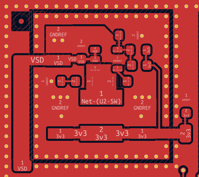
The SMPS section is laid out as a tightly-coupled island that follows the MPS EMI webinar containment pattern. Placement runs U2 → L1 along the SW copper pour, with input decoupling above U2 and the output filter flanking the inductor.
- Two-tier input decoupling. C4 (100 nF HF bypass) sits 2.62 mm from U2 VIN; C2 (10 µF bulk) sits on the outer side at 5.04 mm. C4's GND pad and U2's GND pin share the priority-1 tight GNDREF pour, so the input hot loop is small.
- SW node as copper pour. Net-(U2-SW) is implemented entirely as a high-priority copper pour (priority 50, the highest on the board) spanning from U2's SW pin to L1's input pad — effectively zero trace inductance. C11 (BST cap) sits inside this pour, bridging the CB and SW pins directly. R13/C10 (snubber, both DNP) sit at the south edge of the SW pour, accessible for post-bring-up population.
- Symmetric output filter. C14 and C15 (10 µF each) flank L1 at equal distance (±4.12 mm) on the same axis. This minimises the output ripple-current loop area and shields L1's stray near field. C13 (100 pF rail bypass) sits right at the FB1 input pad.
- Single-bead domain boundary. FB1 is the only copper bridge between the SMPS 3v3 pour and the VCC digital zone — no trace, via, or pour bypass crosses it.
Four-layer GNDREF strategy — moated island plus VCC plane pair
The four-layer stack-up (1.6 mm, ENIG, dark-blue mask) does two different jobs depending on location. Inside the SMPS section (and the matching CAN-power and wind-LDO sections elsewhere on the board), all four layers are GNDREF, surrounded by a copper-keepout moat that contains return currents. In the digital VCC area, F.Cu and B.Cu are VCC pour instead, sandwiching unbroken GNDREF planes on the inner layers — two VCC↔GND plane pairs that act as distributed bypass capacitance.
Inside the SMPS island
The SMPS section sits inside a copper-keepout moat cut on F.Cu, In1.Cu, and In2.Cu. B.Cu is the only layer that spans the full board uninterrupted — there is no moat on the bottom layer. A perimeter via fence runs along the inside edge of the moat, stitching the inside-moat GNDREF on F.Cu / In1.Cu / In2.Cu down to the continuous B.Cu plane. Additional GNDREF vias at every component GND pad keep the four GNDREF layers tightly coupled wherever return current is sourced.
The four layers in the SMPS island:
| Layer | Role inside the SMPS island |
|---|---|
| F.Cu (top, 17.5 µm) | GNDREF pour inside the moat, plus the SMPS sub-pours: SW (priority 50 — highest on the board), VSD input pour, 3v3 output pour. Three layered GNDREF fills under U2: a priority-1 tight pour directly under the IC, a priority-14 extended pour over U2's passives, and a priority-5 broader fill covering the full SMPS area. |
| In1.Cu (inner, 35 µm / 1 oz) | GNDREF inside the moat. Bounded by the moat keepout ring (also has a separate GNDREF fill outside the moat, but the two are physically isolated on this layer). |
| In2.Cu (inner, 35 µm / 1 oz) | GNDREF inside the moat, same pattern as In1.Cu. |
| B.Cu (bottom, 17.5 µm) | Solid GNDREF spanning the full board — no moat. The global low-impedance return reference; what the via fence stitches the inside-moat layers down to. |
 | 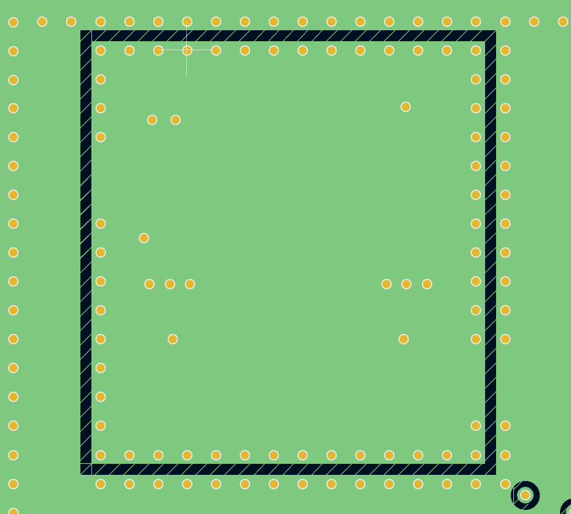 |
| F.Cu — SMPS island | In1.Cu — moat + via fence |
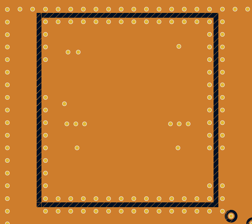 | 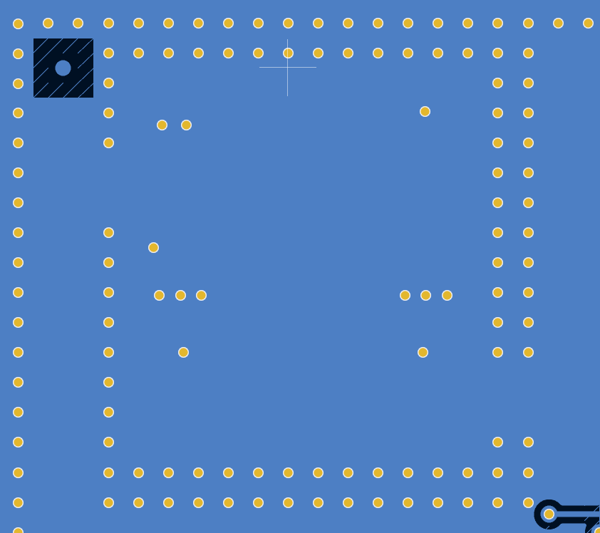 |
| In2.Cu — moat + via fence | B.Cu — full-board GNDREF, no moat |
This is the MPS EMI webinar containment pattern: noisy switching return currents are trapped inside the moat-bounded island on layers 1–3. The only way for them to leave the island is through B.Cu, which adds enough inductance to attenuate high-frequency coupling into the rest of the board. The same moat-and-fence pattern is used around the CAN-bus power section and the wind-transducer LDO section — both are similarly noisy and similarly contained.
In the VCC digital area
The VCC area uses a deliberately different stack-up:
- F.Cu and B.Cu carry VCC pour (not GNDREF).
- In1.Cu and In2.Cu carry unbroken GNDREF (the digital return).
This creates two VCC↔GNDREF plane pairs separated by 0.1855 mm prepreg — an effective distributed bypass capacitor for the VCC rail with no parasitic inductance and no ESR. This is why the moat-bounded GNDREF on F.Cu and B.Cu is only present under the SMPS, CAN-power, and LDO sections: extending it into the VCC area would break the plane-pair capacitance.
Star convergence at U2 GND pad
The feedback divider lower-leg GND return (R1 pad 2), the input cap GND returns (C2, C4), and the bootstrap cap return all converge at U2's GND pin via the priority-1 tight GNDREF pour beneath U2 on F.Cu. There is no long shared via to a distant GND point. This is the "star-point at the IC ground pad" practice from the MPS webinar.
Components
| Ref | Value | Function | Datasheet |
|---|---|---|---|
| U2 | LMR51610XDBVR | Synchronous buck converter, 4–65 V in, 1 A out, SOT-23-5 (DBV), 400 kHz — generates 3.3 V VCC from VSD | TI LMR51610 |
| L1 | 22 µH semi-shielded inductor, 5×5 mm | Production: Bourns SRN5040TA-220M (Isat 1.62 A, Irms 1.50 A, DCR 123 mΩ). Prototype (stock substitute): Fenghua FNR5040S220MT (Isat 1.8 A, Irms 1.6 A, DCR 168 mΩ). See Inductor sourcing. | Bourns SRN5040TA · Fenghua FNR5040 (LCSC) |
| FB1 | BLM31KN601SN1L | 1206 ferrite bead, 600 Ω @ 100 MHz, 80 mΩ DCR — sole copper path from SMPS 3v3 to digital VCC | Murata BLM31KN601SN1L |
| C2 | 10 µF / 50 V X7R 1210 | VSD input bulk capacitor for U2 (Murata GRM32ER71H106KA12L) | Murata GRM32ER71H106KA12L |
| C4 | 100 nF / 50 V X7R 0603 | VSD high-frequency input bypass for U2 (Murata GCM188R71H104KA57D) | Murata GCM188R71H104KA57D |
| C9 | 1 pF / 100 V C0G 0603 | Feedforward capacitor across R2 (3v3 → FB pin); sets a feedback zero | Murata GCM1885C2A1R0BA16D |
| C10 | 1 nF / 50 V C0G 0603 | SW-node snubber capacitor with R13 — DNP by default; fit only if SW ringing observed | — |
| C11 | 100 nF / 50 V X7R 0603 | Bootstrap (CB→SW) capacitor for U2 high-side gate drive — always fitted | Murata GCM188R71H104KA57D |
| C13 | 100 pF / 50 V C0G 0603 | High-frequency 3v3 rail bypass close to L1 output | — |
| C14 | 10 µF / 50 V X7R 1210 | 3v3 output bulk capacitor — left flank of L1 (intentional EMI layout) | Murata GRM32ER71H106KA12L |
| C15 | 10 µF / 50 V X7R 1210 | 3v3 output bulk capacitor — right flank of L1 (symmetric with C14) | Murata GRM32ER71H106KA12L |
| R1 | 32 kΩ 0603 thin film ±0.1 % | Feedback divider lower resistor (sets 3.30 V with R2) | Yageo RC Group |
| R2 | 100 kΩ 0603 thick film ±1 % | Feedback divider upper resistor (3v3 → FB pin) | Yageo RC Group |
| R13 | 22 Ω 0603 thick film ±1 % | SW-node snubber resistor in series with C10 — DNP by default | Yageo RC Group |
| TP1 | — | VCC test point — DNP | — |
Testing & Verification
The V1.2 prototype on the test vessel has been in service for approximately 1,000 sea miles. The VCC SMPS rail powers the ESP32, IMU, button, LED, and pull-ups continuously without observed brownouts or resets in service — but the ESP32 has been running with Wi-Fi never enabled (see operating-context notes elsewhere in these docs), so the SMPS has not yet been loaded by sustained Wi-Fi TX bursts in actual use. No quantitative bench measurements have been performed on the SMPS output voltage, ripple, U2 thermal behaviour, inductor thermal behaviour, or input current under sustained Wi-Fi TX. The following are required.
Hardware bring-up (rig at the bench):
- Output voltage accuracy — Measure VCC at TP1 with no Wi-Fi activity. Pass if 3.30 V ± 2 % (3.234–3.366 V).
- Input current at Wi-Fi TX — Measure VSD-side current at U2 VIN during a sustained 802.11b TX burst (11 Mbps). Pass if mean current is within 130–170 mA at VSD = 12 V.
- U2 IC temperature at sustained Wi-Fi TX — Run continuous 802.11b TX for 10 min at 85 °C enclosure ambient. Pass if U2 case temperature stays below ~95 °C (Tj ≈ 111 °C internal).
- Output ripple at Wi-Fi TX burst — Probe VCC at TP1 with a 100 MHz scope (low-inductance ground, ≤ 5 mm tip-to-tip), sustained 802.11b TX. Pass if peak-to-peak ripple at the 400 kHz fundamental is below 50 mV.
- L1 thermal at sustained load — Touch-probe L1 case after 10 min of continuous Wi-Fi TX at 85 °C ambient. Pass if case is below ~80 °C.
- SW-node snubber decision — Probe SW with a 500 MHz scope (low-inductance ground spring). Pass without snubber if peak ringing is < ~1 V above V_in; otherwise populate R13 + C10.
- VCC vs 3v3 SMPS output, at Wi-Fi TX — Probe both sides of FB1 simultaneously during a Wi-Fi TX burst. Pass if the digital VCC side shows visibly reduced HF ripple compared with the SMPS-output side.
Gaps & next version
Before next production run
- Switch L1 to production BOM — Move from Fenghua FNR5040S220MT (prototype stock) to Bourns SRN5040TA-220M (production); same footprint, ~+0.4–0.5 % efficiency improvement and a guaranteed SRF spec. See Inductor sourcing for the full analysis.
Next version (V1.3)
- Switch U2 to LMR51610XDRGR (DRG package, exposed pad) (if higher MCU or peripheral current budgets anticipated) — DRG θJA = 48 °C/W vs DBV's 148 °C/W. At 180 mW dissipation this gives ΔTj ≈ 8.6 °C vs 26.6 °C — about 18 °C of additional thermal headroom. Same pinout family from TI; minor footprint change.
- Add a per-circuit GNDREF keepout moat around the SW pour (carry forward from MDD400 V2.9) — V1.2 already moats the whole SMPS island, but relies on zone priority alone at the SW node; an explicit 0.4 mm keepout around the SW pour matches the MDD400 V2.9 pattern.
References
- Texas Instruments, LMR516xx SIMPLE SWITCHER® Power Converter, 4 V to 65 V, 0.6 A / 1 A Buck Converter Datasheet — see §8.4 for layout guidance.
- Texas Instruments, Controlling switch-node ringing in synchronous buck converters (SLYT465) — snubber design guidance.
- Texas Instruments, Design Consideration on Boot Resistor in Buck Converter (SNVAA73).
- Murata Electronics, BLM31KN601SN1L Ferrite Bead Datasheet.
- Espressif Systems, ESP32-S3 Datasheet — Table 16, current consumption in active mode.
- Espressif Systems, ESP32-S3-WROOM-1 & WROOM-1U Module Datasheet.
- Monolithic Power Systems, EMI Webinar: Practical Grounding and Layout — the layout reference for this design.
Related pages
- CAN Bus Power — the upstream bus protection chain that delivers VSD to this SMPS.
- Wind Interface — the LP2951 LDO on the same KiCad sheet that supplies the wind transducer.
- ESP32-S3 Module — the dominant VCC consumer this rail is sized for.
- Power Rails — quick-reference summary of every supply rail.