Connectors & Mechanical

CANBench Duo v1.2 — Schematic-stage refresh of the V1.1 fabricated prototype. V1.2 is electrically identical to V1.1 and carries the InvenTree-canonical component metadata; no V1.2 boards exist yet — testing and bring-up reference the V1.1 hardware.
Other versions: v1.1 — fabricated prototype (current)
Overview
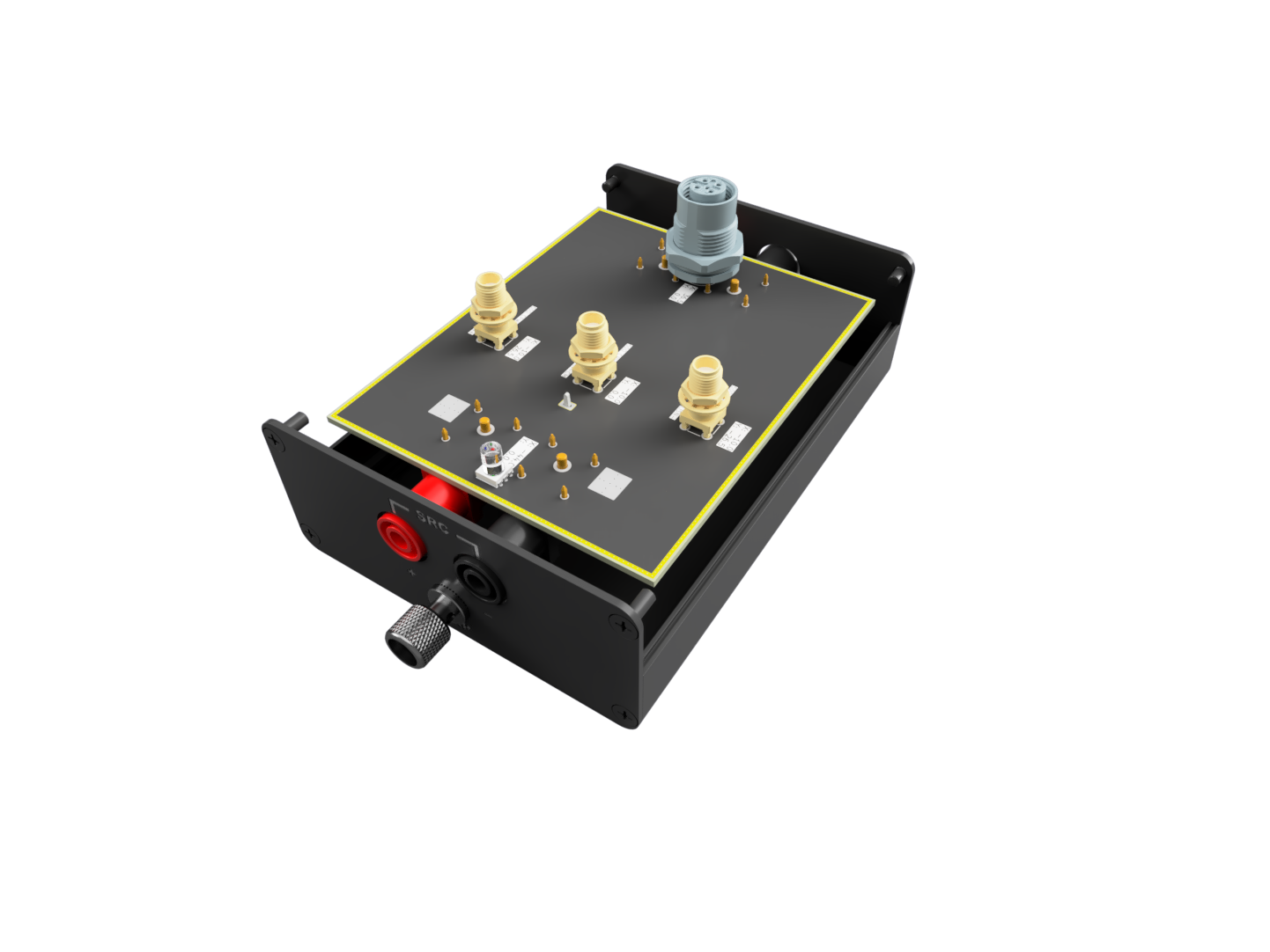
This page covers the connector and mechanical-feature roster for the CANBench Duo, drawn on the connectors_and_mechanical KiCad sheet. It contains no active components, no passive filtering, and no signal conditioning — every component is either a connector that brings an external signal or supply onto the board, or a fiducial that registers the board for pick-and-place assembly.
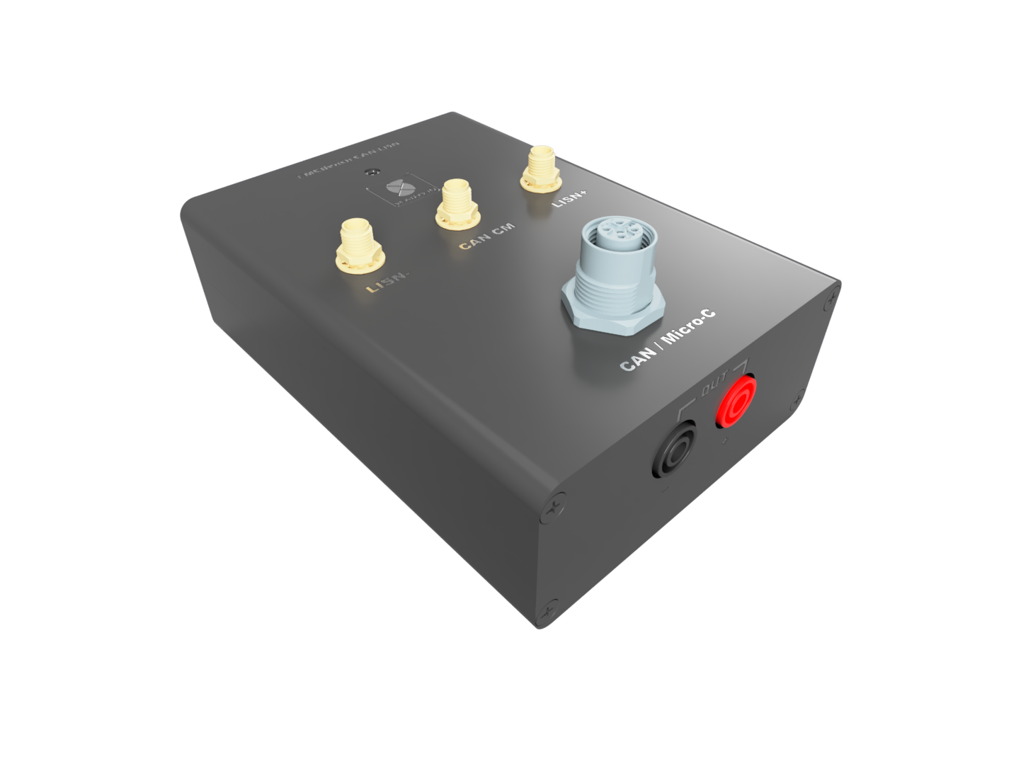
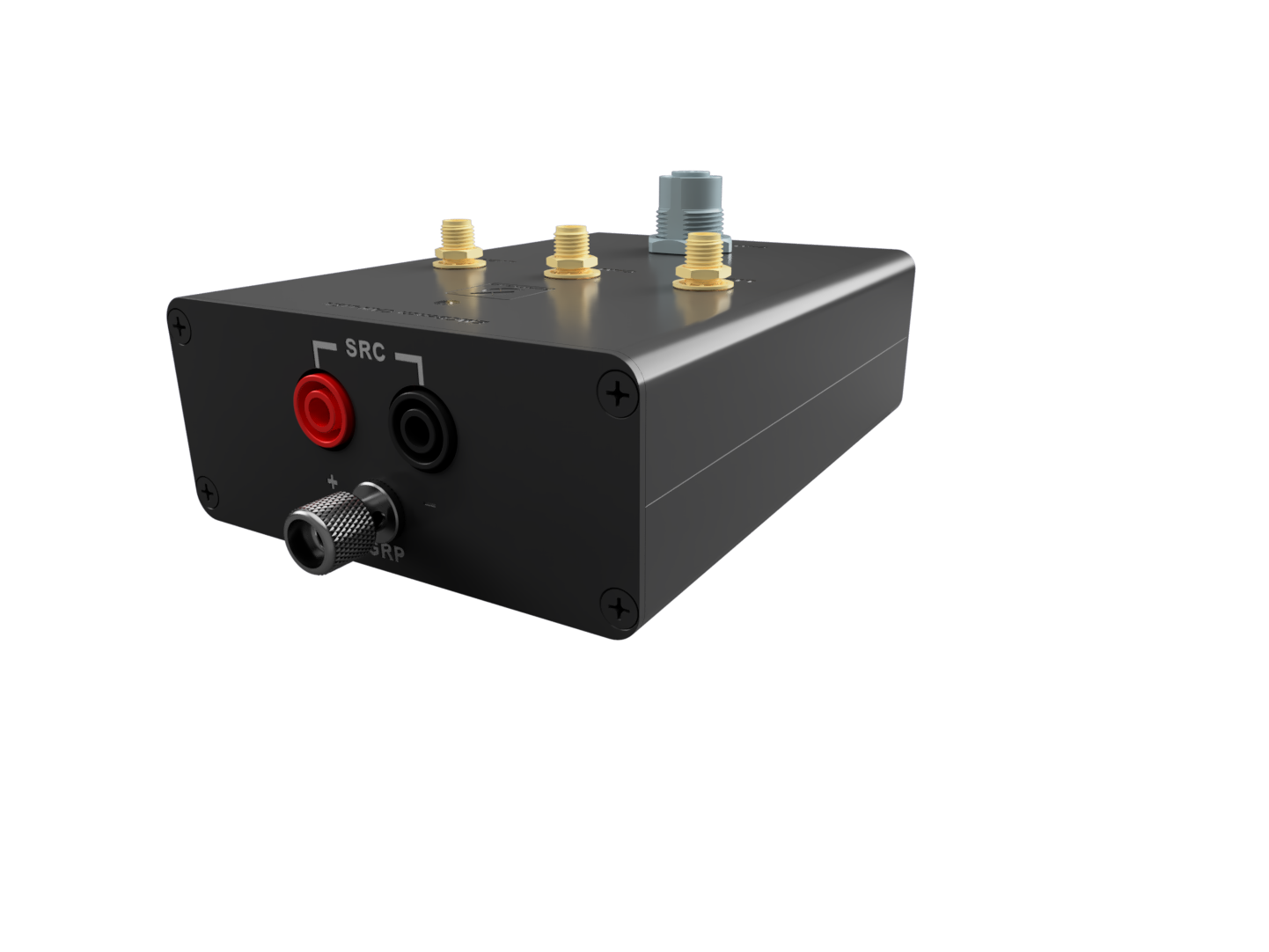
The CANBench Duo uses a dual-face connector layout built around the YG-H10A extruded aluminium enclosure. Three classes of cables come and go: bench supply, DUT supply / N2K, and measurement. Each class emerges from a different face of the enclosure, so all three can lie flat on the test bench without crossing.
| Connector class | Face | Connectors |
|---|---|---|
| Bench supply input | Vertical front faceplate | J5 RED + J7 BLACK banana sockets (SRC) |
| DUT supply / N2K output | Vertical back faceplate + top extrusion | J1 RED + J3 BLACK banana sockets (DUT) + J10 M12-5 N2K |
| Measurement outputs | Top extrusion (B.Cu side) | J2 SMA (LISN+), J4 SMA (LISN−), J6 SMA (CAN-CM) |
Functional specification and design objectives
The connector and mechanical set must:
- bring the bench DC supply onto the board at a clearly polarised SOURCE banana pair (
J5RED /J7BLACK), and deliver the LISN-filtered DC supply back out at a DUT banana pair (J1RED /J3BLACK), with directionality enforced by the internal protection chain so a SRC↔DUT swap is structurally hard to make; - provide a combined NMEA 2000 / DeviceNet supply + CAN-bus interface on a single M12-5 Code A female receptacle (
J10), pin-compatible with the rest of the SCADYS-IO range, delivering the LISN-filtered DC supply and CAN bus on one connector; - present three interchangeable 50 Ω SMA measurement outputs (
J2LISN+,J4LISN−,J6CAN-CM) with a low-inductance shield-to-GNDREF bond, usable across the design's measurement band (150 kHz – 108 MHz) without degrading return loss; - carry the LISN supply path's 4 A continuous @ 25 °C design-intent current through every DC connector and its board traces without exceeding any per-pin rating;
- give the user a tool-free chassis-bond path to the enclosure body; and
- register the board for two-point pick-and-place assembly (fiducials
FID1/FID2).
Measurable targets
| Target | Value |
|---|---|
| Measurement-port characteristic impedance | 50 Ω nominal (J2 / J4 / J6) |
| Measurement band | 150 kHz – 108 MHz (SMA return loss adequate over this band; VNA confirmation at 108 MHz pending) |
| DC connector continuous current | 4 A continuous @ 25 °C (LISN supply path design intent) |
| Banana socket per-pin rating | 10 A (margin over the 4 A design intent) |
| M12 (J10) per-pin rating | 4 A (matches the 4 A design intent — zero margin) |
| SMA DC-through rating | < 500 mA (measurement ports carry RF, not DC supply) |
Connector roster
Banana sockets (J1, J3, J5, J7)
Four Changzhou Amass 24.245.x horizontal edge-mount THT banana sockets — two pairs of RED/BLACK on opposite vertical faceplates:
| Ref | Colour | Net | Face | Role |
|---|---|---|---|---|
J5 | RED | SUPPLY+ | Front | Bench supply positive in |
J7 | BLACK | SUPPLY− | Front | Bench supply negative in |
J1 | RED | DUT+ | Back | DUT positive out (LISN-filtered) |
J3 | BLACK | DUT− | Back | DUT negative out (LISN-filtered) |
Directionality is fixed by the internal LISN protection chain — bench supply enters on the SRC pair, passes through fuse + reverse-polarity protection + ferrite + LISN ladder, and emerges on the DUT pair. Wiring the bench supply to the DUT pair (or DUT to the SRC pair) bypasses the entire protection chain. The Red LED state on the top indicator catches reverse polarity within either pair, but it cannot catch SRC-vs-DUT pair swap.
Banana socket per-pin current rating: typically 10 A continuous for this connector class. The LISN supply path's design intent is 4 A continuous @ 25 °C — well within the socket rating.
SMA measurement outputs (J2, J4, J6)
Three HCTL HC-SMA6565-13H-G SMA Female Vertical THT connectors on the top extrusion, evenly spaced 26.5 mm apart along the X = 110 mm column:
| Ref | Net | Position (X, Y) mm | Role |
|---|---|---|---|
J2 | RF_LISN_P | (110, 116.5) | LISN+ measurement (upper rail) |
J6 | RF_CAN_CM | (110, 90) | CAN common-mode measurement (centre row) |
J4 | RF_LISN_N | (110, 63.5) | LISN− measurement (lower rail) |
All three SMAs are visually and electrically interchangeable — same part number, same pinout (centre pin = signal, outer = GNDREF), same characteristic impedance (50 Ω nominal). The HCTL part is rated to typically 12–18 GHz with VSWR ≤ 1.3:1 to 6 GHz, comfortably above the design's 108 MHz upper measurement-band edge. For certification-quality measurement work, validate the actual return loss at 108 MHz via VNA on the as-built board.
M12 N2K connector (J10)
A single Shenzhen STA M12-S5A-PPFM panel-mount female receptacle following the standard NMEA 2000 / DeviceNET Micro-C 5-pin Code A pinout:

| Pin | Net | Standard mapping |
|---|---|---|
| 1 | GNDREF | SHIELD |
| 2 | DUT+ | NET-S (V+) |
| 3 | DUT− | NET-C (V−) |
| 4 | NET-H | CAN-H |
| 5 | NET-L | CAN-L |
J10's pins 2 / 3 tie to the same DUT+ / DUT− nets as the back-faceplate banana pair, so a DUT plugged into J10 via a standard N2K cable receives the LISN-filtered DC supply AND the CAN bus on the same connector. This matches the way N2K-attached devices receive power and connectivity from the backbone cable. The pinout is identical to the SCADYS-IO platform's MDD400 / WTI400 / MLI400 / MDG400 — any of those products can be powered + bussed via the CANBench Duo's J10.
The M12-S5A-PPFM is rated 4 A per pin, which matches the LISN supply path's 4 A continuous design intent exactly. Zero margin. For DUT currents up to 4 A continuous J10 is acceptable; for higher currents, use the back-faceplate banana pair (J1/J3, ~10 A rated) instead — at the cost of CAN-bus connectivity, which then has to be cabled separately.
The M12 connector form factor is N2K-compatible and the pinout follows the NMEA 2000 standard, but the CANBench Duo itself is a measurement instrument — it does not carry the N2K logo or certification. The IP67 rating is a side effect of using the standard N2K connector class, not a marine-deployment claim. This is a bench instrument.
Chassis-ground binding post
A wire braid runs from the PCB GNDREF (at the J8 Keystone pad position on F.Cu) to a knurled-knob binding post on the front faceplate, visible in render_2.PNG. The J8 PCB pad itself is (dnp yes) — the chassis bond uses the external binding post instead, which gives the user a tool-free way to bond the enclosure body to an external ground rod or test-bench ground.
The binding post is the primary chassis-bond path on V1.1 / V1.2. Future revisions may populate J8 directly if a screw-down stud bond proves preferable in the field.
Fiducials (FID1, FID2)
Two pick-and-place fiducial marks at diagonally opposite corners of the PCB — FID1 at the top-left, FID2 at the bottom-right. Used by the assembly machine's vision system for two-point board registration. No user-facing role.
Mechanical orientation
The PCB sits inside the YG-H10A extruded aluminium enclosure with the following orientation (see canbench-duo-enclosure-orientation memory for the canonical reference):
- B.Cu (with the SMAs, M12, and indicator LED) faces UP through the top extrusion cutouts
- F.Cu (with the bananas, fiducials, and silkscreen markings) faces DOWN against the GRP test bench
- Banana sockets emerge horizontally through the vertical front + back faceplates
- The chassis-ground binding post protrudes from the front faceplate next to the SRC banana pair
This orientation is unusual compared to many bench instruments where everything is on a single front face. The motivation is cable layout: measurement cables emerging upward from the top let the SMA cables drape naturally; the front + back banana pairs let bench-supply and DUT cables enter from opposite sides without crossing the SMA cables. The instrument lies flat on the GRP bench surface with all cables in their natural orientation.
PCB Layout
The connectors are placed for whole-board mirror symmetry across the Y = 90 mm axis — the same axis that mirrors the LISN supply path's ladder, protection FETs, and measurement-port chains. The board is 99 × 79 mm (X = 70.5–169.5 mm, Y = 50.5–129.5 mm).
- Banana sockets on the front face (F.Cu), split left/right by signal flow. The SOURCE pair (J5 RED, J7 BLACK) sits on the left edge at X = 71.5; the DUT pair (J1 RED, J3 BLACK) on the right edge at X = 168.5. Each pair straddles the Y = 90 mirror axis at Y = 99.5 / 80.5 (19 mm apart). This is a deliberate left-in / right-out layout — bench supply enters left, LISN-filtered output emerges right — so the sockets are on the same face but opposite edges.
- SMA verticals on the back face (B.Cu), aligned in the X = 110 column at Y = 116.5 (J2 LISN+), Y = 90 (J6 CAN-CM), Y = 63.5 (J4 LISN−), evenly spaced 26.5 mm apart. J2/J4 mirror across Y = 90; the TVS-to-SMA traces are inherently length-matched by that mirror geometry. The SMAs emerge through the top extrusion, separated from the front-face bananas.
- M12 (J10) on the back face at (156.5, 90), on the Y = 90 axis, right of centre — a separate face from the bananas.
- Chassis-ground stud (J8, DNP) on F.Cu at the board centre (100, 90); the GNDREF pad is placed even though the part is not populated, so a field-time install works.
- Fiducials at diagonally opposite corners: FID1 at (73.5, 126.5) top-left, FID2 at (166.5, 53.5) bottom-right — both ~3 mm in from the corner, clear of connector bodies that could shadow the vision system.
- Ground continuity: a continuous B.Cu GNDREF flood runs beneath all connector positions, providing the reference plane for the SMA shields (J2/J4/J6 pin 2) and the M12 shield (J10 pin 1). The enclosure bond relies on the SMA shells plus the M12 shield, since J8 is DNP.
See pcb_review/connectors-and-mechanical-layout.md in the source repository for the full per-component coordinate table and verification against the schema-review's layout requirements.
Connector specifications
| Connector | Manufacturer / MPN | Rating | Mating cycles | IP rating |
|---|---|---|---|---|
| Banana sockets (J1/J3/J5/J7) | Changzhou Amass 24.245.1 (RED) / 24.245.2 (BLACK) | 10 A | 5 000+ | None |
| SMA Female Vertical (J2/J4/J6) | HCTL HC-SMA6565-13H-G | 50 Ω, 12–18 GHz, < 500 mA DC | 500+ | None |
| M12 N2K (J10) | Shenzhen STA M12-S5A-PPFM | 4 A per pin | 100+ | IP67 (connector class) |
| Chassis-ground binding post | YIYUAN YTC-3-PCB281308 (J8 pad, DNP) — wire braid to enclosure post | High-current | One-time install | N/A |
Components
| Ref | Value | Function | Datasheet |
|---|---|---|---|
| J5 | 24.245.1 (RED) | Banana socket, horizontal edge-mount THT — bench-supply positive input (SUPPLY+) | Changzhou Amass 24.245.1 |
| J7 | 24.245.2 (BLACK) | Banana socket, horizontal edge-mount THT — bench-supply negative input (SUPPLY−) | Changzhou Amass 24.245.2 |
| J1 | 24.245.1 (RED) | Banana socket, horizontal edge-mount THT — DUT-side positive output (DUT+) | Changzhou Amass 24.245.1 |
| J3 | 24.245.2 (BLACK) | Banana socket, horizontal edge-mount THT — DUT-side negative output (DUT−) | Changzhou Amass 24.245.2 |
| J2 | SMA_Female_Vertical | SMA Female vertical THT, 50 Ω — LISN+ measurement port (RF_LISN_P) | HCTL HC-SMA6565-13H-G |
| J4 | SMA_Female_Vertical | SMA Female vertical THT, 50 Ω — LISN− measurement port (RF_LISN_N) | HCTL HC-SMA6565-13H-G |
| J6 | SMA_Female_Vertical | SMA Female vertical THT, 50 Ω — CAN common-mode measurement port (RF_CAN_CM) | HCTL HC-SMA6565-13H-G |
| J10 | N2K_Female | M12-5-pin Code A female panel-mount, IP67 — combined DUT supply + CAN bus | Shenzhen STA M12-S5A-PPFM |
| J8 | 1211 (DNP) | Keystone 1211 quick-terminal — reserved chassis-ground stud, not populated | YIYUAN YTC-3-PCB281308 |
| FID1 | Fiducial | Pick-and-place registration mark (top-left corner) | — |
| FID2 | Fiducial | Pick-and-place registration mark (bottom-right corner) | — |
J9 is intentionally absent from the refdes sequence — no J9 symbol exists on this sheet or anywhere in the project. The gap is an artefact of refdes renumbering during the V1.0 → V1.1 → V1.2 evolution; references are reassigned but never reused.
Gaps & next version
Before next production run
- High-current trace widths for the
SUPPLY±/DUT±/VSS±/VSF±nets are not yet verified against IPC-2152 for the 4 A continuous design intent. Board-level minimum track width is 1.0 mm; IPC-2152 indicates ~ 1.5 mm at 4 A continuous, 30 °C rise on 1 oz outer-layer copper. - HCTL HC-SMA6565-13H-G return loss at 108 MHz is not characterised in the manufacturer datasheet. Adequate for pre-compliance work; VNA confirmation pending for certification-grade measurement.
- SMA / M12 ground-via cluster density is sparse around the connector shells — a recurring observation across the PCB reviews. Either add via stitching or verify ESD / RF chassis-bond performance.
Next version
- High-current trace-width respin — widen the
SUPPLY±/DUT±rails to the IPC-2152 figure above; a V1.3 candidate. - J8 chassis-ground stud — decide whether to populate J8 for a dedicated screw-down chassis bond, or leave it DNP and keep relying on the SMA shells + M12 shield + external binding post.
References
- Changzhou Amass Electronics, 24.245.1 RED banana socket, horizontal edge-mount THT (J1, J5)
- Changzhou Amass Electronics, 24.245.2 BLACK banana socket, horizontal edge-mount THT (J3, J7)
- HCTL, HC-SMA6565-13H-G SMA Female Vertical 50 Ω THT (J2, J4, J6)
- Shenzhen STA Electronics, M12-S5A-PPFM 5-pin Code A female panel-mount IP67 (J10)
- YIYUAN, YTC-3-PCB281308 Keystone 1211 quick-terminal (J8, DNP)
- NMEA, NMEA 2000 Standard — Micro-C 5-pin Code A pinout for J10
- IEC 62680-1-3 — DeviceNet physical layer (same Micro-C pinout family)
Related pages
- LISN Supply Path — the fuse, reverse-polarity FET pair, ferrite, and LISN ladder that sit between the SRC and DUT banana pairs
- LISN Measurement Ports — the RF chains driving the LISN+ / LISN− SMAs (J2 / J4)
- CAN Common-Mode Port — the RF chain driving the CAN-CM SMA (J6) and tapping J10's pins 4 / 5
- Power Indicator LED — the indicator visible through the top extrusion
- User Manual → Quick Start — operational workflow including cable-layout conventions; Quick Reference → Connectors — connector roster lookup table